
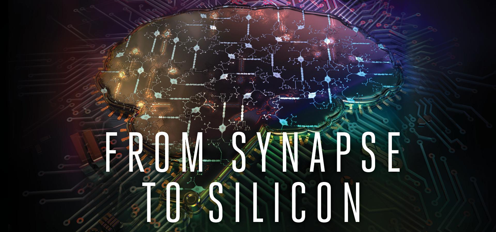
From Synapse to Silicon
GW researchers are on the forefront of a revolution in computer hardware innovation—designing and fabricating computer chips that take inspiration from the human brain.
Story // Sarah C.P. Williams
Art and Animation // Sayo-Art LLC
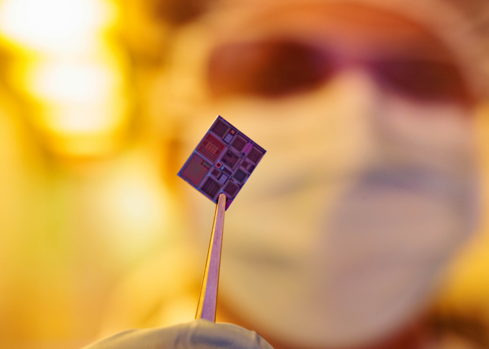
In the palm of his hand, Lei Zhang, a fourth-year electrical engineering doctoral student, holds a square computer chip. It’s small enough that when he covers it with the tip of a finger, it disappears. To the naked eye, it looks like any other microchip—it began as a wafer of silicon, on which millions of microscopic wires and electrical components were created by successively depositing and carving away thin layers of material. But the chip designed by Zhang has a special use: To be part of an interconnected network of chips, in a future implantable device, that can detect the heart’s electrical signals, differentiate a healthy heartbeat from an abnormal one, and trigger tiny electrical pulses to coax the heart’s abnormal rhythm back into its usual lub-dub-lub-dub rhythm.
Most devices that can analyze a person’s heart function and help maintain a normal heartbeat are larger—the size of at least a penny for simpler heartbeat analysis or much larger, such as a wearable vest, for more complex cardiac mapping. These devices also require multiple microchips to process and store data. Zhang’s device, though, is so small that dozens of them could be implanted onto the surface of a human heart at once to deliver precisely coordinated shocks from all directions. That is in part because some of its underlying technology takes inspiration from one of the most energy-efficient and powerful computers known to mankind: the human brain.
“This is a completely new generation of technologies, and they’re useful for all kinds of applications beyond just real-time sensing and therapy in the human body,” says Zhang. “And GW is one of the best places to be working on this.”
Computer chips are the basis for nearly every electronic device produced today. The tiny circuits that compose them can carry out computations, make decisions and store information. Simple chips power the repetitive reasoning of a calculator; more complex combinations of chips let massive computer systems learn how to predict the weather, the direction of tomorrow’s stock market, how millions of human genes are associated with a disease or the potential origins of a new virus, like COVID-19.
At GW’s School of Engineering and Applied Science, researchers are trying to push the limits of how fast and efficiently computer chips can operate. One of their tactics is designing chips that function more like a living brain. Their work has implications in not only shrinking and speeding up consumer devices like cell phones and smart watches but also in allowing powerful artificial intelligence (AI) programs to run more quickly and smoothly—a major change that could revolutionize fields from economics to health care.
“Right now, there are tasks that humans are still much better than computers at,” says Tarek El-Ghazawi, chair of electrical and computer engineering at GW. “The brain can analyze things brilliantly, weighing all kinds of information to make decisions, while consuming almost no power. How can we mimic this in computer hardware?”

The memristor-based microchip seen here is being designed to differentiate a healthy heartbeat from an abnormal one and trigger electrical pulses to coax the heart back into its normal rhythm.
Electrical engineering doctoral student Lei Zhang designed the memristor-based microchip to be part of a network of chips that could be implanted on the heart.
A standard computer chip has billions of transistors on its surface; these vast networks of on-off switches shuttle streams of electrons through large, complex circuits. Everything you see and hear on an electronic device is encoded in the on-off states of those transistors—represented as 0s and 1s in computer language.
“The computer chip is one of the most advanced and astounding things that humankind has created,” says Gina Adam, an assistant professor of electrical and computer engineering whose lab is developing next-generation computing hardware. “It amazes me that this feat of engineering is just everywhere in our lives today.”
In recent decades, electrical engineers have shrunk, again and again, the size of transistors. In 1947, a single transistor measured a few millimeters across; by 1990, it was less than a micrometer (at least ten times smaller than the width of a single human hair). Today, the transistor channel has shrunk down to a few nanometers—a nearly unfathomable size of just a few atoms. This downsizing has allowed chips and, in turn, computing systems to become smaller and more powerful.
Today’s transistors, however, are nearly as small as they can possibly be—any smaller and they wouldn’t be able to physically control the electrons that must pass through them. Researchers have also discovered that the tiniest transistors tend to have flaws; they fail more often and, packed together by the billions, can generate immense heat (this explains why your cellphone feels warm after a long call).
“We’re approaching the physical limits of how small we can make transistors using current technologies,” says El-Ghazawi. “But every time people think we have reached a limit, someone comes up with a new trick to extend the life of an existing technology or create a new enabling technology altogether.”
Even if transistors can’t be made smaller, he says, electronic circuits made out of transistors can still be organized in new architectures to make chips more powerful. In addition, many researchers are innovating new specialized devices as helpers to stack on top of computing chips—these so-called accelerators can use different innovative ways of processing and storing data to boost the power of existing chips.

“We’re approaching the physical limits of how small we can make transistors using current technologies. But every time people think we have reached a limit, someone comes up with a new trick to extend the life of an existing technology or create a new enabling technology altogether.”
– Tarek El-Ghazawi, Chair and Professor of the Electrical and Computer Engineering Department
The accelerators and chips that Adam designs move beyond the transistor technology of 0s and 1s. Today, computing systems generally process information on one chip (a processor) and store large amounts of information on another chip (the memory). Moving data between these chips requires time and energy.
“It’s been very challenging because as processors have become faster and memories have become bigger, there are a lot of mismatches; the processor needs to constantly wait to fetch data from the memory,” explains Adam, a National Science Foundation CAREER Awardee and recipient of the Young Investigator Program Award from the Air Force Office of Scientific Research. “But in the human brain, we don’t separate memory into a different area. The same neuronal circuitry that processes information also stores it.”
Adam is collaborating with neuroscientists to better understand how the brain accomplishes this and how different neurons and supporting cells function and connect.
“We want to know why there is so much diversity of cell types in the brain, and how much of this diversity needs to be translated into our devices and neuro-inspired hardware systems,” she says.
Now, Adam is using her neuro-know-how to build new types of devices that eliminate the distance between the processor and memory. Among those devices are memristors, short for “memory resistors,” which behave like artificial synapses by “remembering” the amount of electric charge that has passed through them.
Rather than moving electrons as transistors do, memristors involve the rearrangement of ions. Ions are charged atoms, much larger than electrons. When an electric current is applied to a memristor, heat is generated and those bulky ions start to move. As they move, the internal structure of the memristor changes, modifying its resistance value—how much the device resists the flow of electrical current. When the heat is removed, the ion motion halts, yet the new structure of the memristor freezes in place, giving the device a new resistance value. With each change in resistance, ions flow through the device differently when an electric current is applied again.
From Synapse to Silicon
Information is encoded in the brain and memories are made when an electrical signal repeatedly spurs the release of neurotransmitters (blue dots) across a synaptic gap between neurons, strengthening the connection between those neurons (pink) and making it easier to recall information. Similarly, information is encoded and stored on a memristor chip when an electrical current reconfigures a filament of titanium dioxide (blue dots) between two electrodes, which changes the resistance value of the device so that it “remembers” the charge that passed through it previously.
“What this means is that a memristor can actually learn. Like synapses in the brain, it changes gradually based on signals it has received,” says Adam.
It also means that a memristor synapse can communicate in shades of gray, strengthening or weakening the connections between artificial neurons, rather than being limited to the black-and-white 0s and 1s of transistors. A memristor has numerous states, each subtly different, depending on the arrangement of ions in its structure.
What does this look like at a practical level? Memristors could contribute to faster, more powerful data processing, computers that don’t lose information when they shut down, and systems—like Zhang’s implantable chip for the human heart—that can work for years, consuming little battery power. Their resemblance to a human brain, with shades of gray and memory integrated into processing, also means they are useful for the massive computing power needed in AI and machine learning platforms that aim to mimic human learning and reasoning.
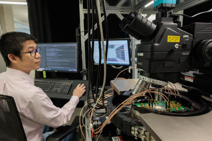
Another member of the Adam lab—third-year doctoral student Imtiaz Hossen—designs and fabricates memristors in the GW Nanofabrication and Imaging Center’s (GWNIC) cleanroom, a state-of-the-art facility that houses the equipment needed to produce novel devices and computer components. A small square chip he holds in his tweezers—nearly identical in appearance to Zhang’s chip—has 20,000 tiny memristors on it.
“The way these 20,000 memristors behave gives us really important information,” says Hossen. “But we’ll actually want to scale the system up to the range of a million memristors on a chip or more for real-world applications. That translates to more storage and more data analysis capabilities.”
Third-year doctoral student Imtiaz Hossen shows off a microchip, on which 20,000 memristors have been integrated.

Hossen (left) and Adam (right) have been fine-tuning the design and fabrication of memristor devices to be compatible with the chip underneath. Other lab members then test the chip with the integrated memristors.

The memristor (center) sits between two electrodes that connect to transistors on a chip by way of circular “vias,” or vertical electrical connections.
Hossen has been fine-tuning the design and fabrication of these memristor devices so that they mesh perfectly with a chip underneath. Now he’s begun handing off the chip with integrated memristors for testing by other lab members.
In 2022, GW became one of five academic research centers to partner with the National Institute for Standards and Technology (NIST), Google and chip manufacturer SkyWater Technologies to create a new supply of chips for research and development. As part of the agreement, SkyWater will fabricate test chips based on designs from Adam’s team and the other academic partners and ship them to researchers in the broader community who will integrate their own memristor or other emerging device technologies. They can then use the chips to test how memristors or other accelerator devices work in conjunction with the standard transistor technology.
“This lets us benchmark technologies,” says Adam. “We have the same underlying hardware, the same software, the same codes, and we can test how different devices stack up against each other.”
NIST, the national lab affiliated with the Department of Commerce that’s just a short drive from GW, helps lead and coordinate much of the new CHIPS Act initiatives aimed at supporting computer chip innovation in the U.S. It’s these types of university-industry-government collaborations that drew Adam to GW.
Ahmed Louri, the David and Marilyn Karlgaard Endowed Chair Professor of Electrical and Computer Engineering, also draws inspiration from the human brain in his research and collaborates with neuroscientists around the country who study the inner workings of the hippocampus—the brain’s center of emotion and memory. Already, computer algorithms called neural networks try to mimic the structure and functioning of the hippocampus to make decisions and recognize patterns. But processing such algorithms requires a significant amount of processing power and consumes excessive energy.
"What we want to do is design chips that optimize how neural networks can run efficiently," says Louri, who has dedicated his career to developing high-performance, energy-efficient, and versatile AI chips. "That means emulating the brain in functionality with much higher speed and energy efficiency: Neurons become processing elements, synapses that connect the neurons become physical wires, and the way these processing elements are connected at the physical level is completely different from that in conventional chips."
Louri envisions an ideal AI chip, which he calls a versatile machine learning accelerator, that can execute a targeted class of AI applications much faster and with much less energy, similar to how a Swiss Army knife has many tools for specific tasks. However, unlike the Swiss Army knife, in which only one tool is used at a time, Louri’s chip will be able to execute multiple applications simultaneously. He has developed novel chip interconnects to speed up data movement between processing elements and memory modules while minimizing energy consumption. Supported with several National Science Foundation awards, the chip interconnects have demonstrated exceptional adaptability for running diverse applications and, says Louri, are considered a promising solution for next-generation chips by an industry consortium led by major semiconductor companies.
Louri, an IEEE Fellow who received the IEEE Computer Society 2020 Edward J. McCluskey Technical Achievement Award and the Distinguished Researcher Award from GW’s Office of the Vice Provost for Research in 2021, wants to design computer chips and hardware that are more eco-friendly.

A paper by Louri and doctoral student Jiaqi Yang, “Venus: A Versatile Deep Neural Network Accelerator Architecture Design for Multiple Applications,” was accepted for the 2023 Design Automation Conference in California.
Louri is also exploring incorporating other emerging technologies, such as silicon photonics, which use light instead of electrons to encode information, into AI chips. He’s developed photonic architectures that seamlessly connect numerous processing elements, an approach that allows for scaling the processing power to be on par with the human brain while consuming orders of magnitude lower energy compared to existing electronic chips.
Some of Louri’s motivation is driven by the need he sees for eco-friendly technology. Today, the energy consumption of computing devices and systems accounts for a significant percentage of global carbon emissions.
"Our world increasingly relies on digital systems and computer chips to record, support and shape most aspects of human activity, from commerce to transportation, from health to social networks, from experimental sciences to numerical engineering, and from manufacturing to knowledge production," he says. “This means there are vast opportunities to improve chips and their efficiency. There is no better time than right now for the field of computer engineering.”
That excitement is echoed by El-Ghazawi, who says the growth and innovation around chip design and fabrication in his department are evidence of GW’s growing strength in this field. In addition to his own research and that of Louri and Adam, he points to the pioneering work of other faculty such as Mona Zaghloul and Guru Venkataramani.
“Together faculty research in this area has been funded by millions of dollars and produced scores of patents and publications,” El-Ghazawi says.
”There are vast opportunities to improve chips and their efficiency. There is no better time than right now for the field of computer engineering.”
– Ahmed Louri, David and Marilyn Karlgaard Endowed Chair Professor of Electrical and Computer Engineering
In the U.S., speeding up computer chips has become a national priority, as evidenced by the estimated $280 billion investment in the CHIPS and Science Act passed by Congress and signed into law by President Biden in 2022.
“There’s been a major drive right now to bring back chip manufacturing capabilities to the U.S. rather than contract them out to other countries,” says El-Ghazawi. “Scientists believe that advances in these kinds of technologies will actually determine the next global superpower.”
The CHIPS Act was inspired by the fact that only about 14% of all semiconductors—the fundamental materials of chips—are currently manufactured in the U.S., a drastic drop from the 37% of semiconductors made here in 1990. The act includes direct funding for research like that carried out at GW but also money to support new chip manufacturing facilities and to invest in education related to semiconductor research, development and manufacturing.
“This is going to create tremendous opportunities for our electrical and computer engineering students,” says El-Ghazawi, referring to the push for new jobs in the semiconductor industry.
GW’s Nanofabrication Center is helping students—from interested high schoolers to students at GW—learn the nuts and bolts of this industry, including how to collaborate with researchers in other fields.

Picture left: Doctoral student Juliana Curry with Louri at the High Performance Computing Architectures and Technologies Lab. Picture right: Hossen, Adam and Zhang in the Adaptive Devices and Microsystems Lab.
It’s what allowed Zhang—under Adam’s mentorship—to design his chips for future cardiac implants.
He and Adam collaborated with Igor Efimov, a professor who specializes in cardiovascular engineering and who recently moved from GW’s biomedical engineering department to Northwestern University. Together they are working to design the appropriate algorithms and memristor chips for future testing on heart tissue. While still experimental, their proposed system has already shown 96% accuracy at detecting abnormal heart rhythms.
For Adam, who credits her early teachers in Romania with inspiring her to pursue science, the work with Zhang and Efimov demonstrates how critical both mentorship and partnership are to science.
“I was fortunate to have amazing mentors throughout my education, and my goal is to pay that forward,” she says. “I want students to not only be able to learn the science and engineering concepts but also how to get along with and collaborate with people in diverse fields and from diverse backgrounds.”
Photography: William Atkins